



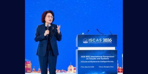
New semiconductor framework unveiled at IEEE ISCAS 2026 focuses on time-based scaling, LogicFolding architecture, and system-level optimisation to drive future AI and computing performance.
Shanghai — Huawei has introduced a new semiconductor development framework called the Tau (τ) Scaling Law, positioning it as a potential successor to traditional geometric scaling approaches that have guided the chip industry for decades.
The announcement was made on May 25 during the 2026 edition of the IEEE International Symposium on Circuits and Systems, where He Tingbo, Director, Chair of Huawei Scientist Committee, ITMT Director, and President of Huawei’s Semiconductor Business Department, delivered a keynote titled “New Semiconductor Path in Practice.”
The Tau (τ) Scaling Law proposes replacing conventional geometric scaling with time-based scaling as the core principle guiding semiconductor and electronic system evolution. Instead of focusing solely on shrinking transistor size, the framework prioritises compressing signal propagation delay and reducing execution time across devices, circuits, chips, and systems.
Industry observers and peers have also begun informally referring to the framework as “Her’s Law” in recognition of He Tingbo’s role in advancing the concept.
For more than five decades, the semiconductor industry has relied on Moore’s Law, which predicted the doubling of transistor density over time. However, the sector is increasingly facing physical limitations, rising fabrication complexity, and diminishing economic returns from further transistor miniaturisation. Huawei argues that the τ Scaling Law offers an alternative pathway to sustain semiconductor innovation while addressing surging global computing demands.
According to Huawei, the new framework is supported by a range of architectural innovations, including LogicFolding, a technology designed to significantly shorten critical-path wiring and reduce resistive and capacitive loads in circuits.
The company outlined how the τ Scaling Law is applied across multiple layers of semiconductor design:
- At the device level, Huawei is optimising transistor resistance and parasitic capacitance to minimise physical-layer time constants.
- At the circuit level, the LogicFolding architecture aims to break traditional layout limitations and improve transistor density and circuit performance.
- At the chip level, Huawei is adopting full-stack co-design across software, architecture, and silicon to improve workload efficiency and reduce execution time.
- At the system level, the company is redesigning interconnect protocols through UnifiedBus technology to reduce communication latency and enable unified memory semantics for large-scale computing systems.
Huawei revealed that over the past six years, it has designed and mass-produced 381 chips based on principles aligned with the τ Scaling Law, supporting a broad range of applications and markets.
The company also disclosed that its upcoming Kirin chips, scheduled for launch in Fall 2026, will be the first to incorporate the LogicFolding architecture. Huawei claims the design will deliver significant performance improvements.
Looking further ahead, Huawei stated that by 2031 its high-end chips developed using the τ Scaling Law are expected to achieve transistor density levels comparable to 14 Å (1.4 nm) process technologies.
During her keynote, He Tingbo emphasised that collaboration across the global semiconductor ecosystem would be critical to sustaining innovation in the post-Moore’s Law era.
“We believe that openness and collaboration are key to driving ongoing progress in the semiconductor industry. No single company can independently find all the answers along the path of semiconductor evolution,” she said.
Huawei added that it intends to work closely with scientists, engineers, and industry partners worldwide to advance sustainable semiconductor and electronics development.